- 您现在的位置:买卖IC网 > Sheet目录2007 > LTC6991MPS6#TRPBF (Linear Technology)IC OSCILLATOR RESET LF TSOT23-6
LTC6991
11
6991fb
OPERATION
RST Pin and Polarity (POL) Bit
The RST pin controls the state of the LTC6991’s output
as seen on the OUT pin. The active/inactive voltage levels
depend on the POL bit setting.
Table 2. Output States
POL BIT
RST PIN
OUTPUT STATE
0
Oscillating
0
1
0 (reset)
1
0
1 (reset)
1
Oscillating
Each period of the LTC6991’s internal oscillator clocks the
output state latch (see Block Diagram). The reset pin (RST)
can reset or hold off the output latch. The active state of
the reset pin is determined by the polarity function (POL).
Similarly, the output latch is followed by a buffer that can
invert the output. The output polarity is also controlled
by the POL bit.
If POL = 0, the reset pin is active high and the output latch
is not inverted. Therefore, pulling the RST pin high will
reset the output latch and force the OUT pin low. Pulling
RST low will allow the output to oscillate, with the next
rising edge dependent on the internal oscillator.
If POL = 1, the reset pin is active low and the output latch
is inverted. Therefore, pulling the RST pin low will reset
the output latch and force the OUT pin high. Pulling RST
high will allow the output to oscillate, with the next falling
edge dependent on the internal oscillator.
Note that the master oscillator frequency and phase are not
affected by the RST pin; The LTC6991 continues to oscil-
late, internally, even when RST is active. While the reset
function can block an output pulse, its exact placement in
time can only be changed by power cycling the LTC6991.
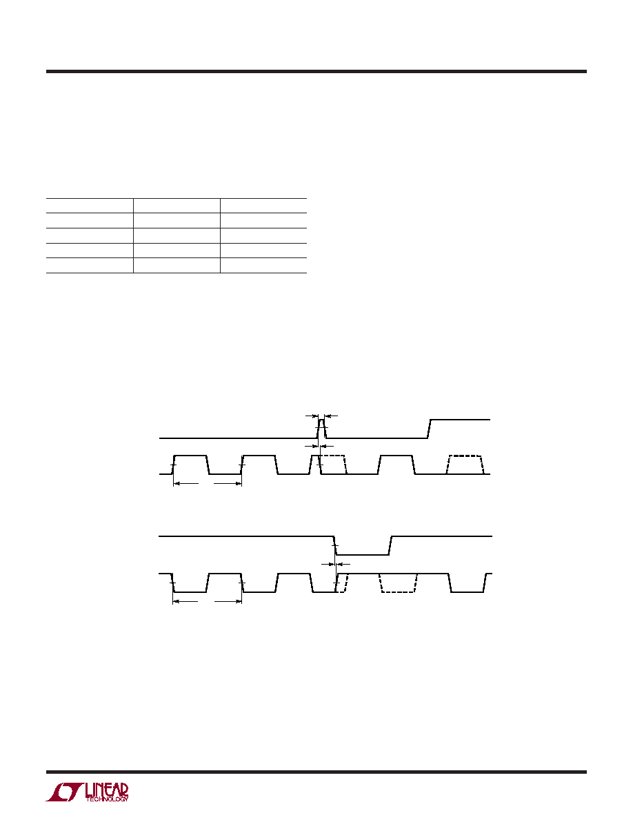
tOUT
RST
OUT
tRST
tWIDTH
INTERNAL
OSCILLATOR
6991 F03
tOUT
RST
OUT
tRST
INTERNAL
OSCILLATOR
6991 F04
Figure 3. RST Timing Diagram (POL = 0)
Figure 4. RST Timing Diagram (POL = 1)
发布紧急采购,3分钟左右您将得到回复。
相关PDF资料
LTC6992MPS6-4#TRPBF
IC OSC PWM VOLT CTLR TSOT23-6
LTC6994CDCB-2#TRPBF
IC DELAY LINE 6-DFN
LTC7541ABN#PBF
IC CMOS D/A CONV 12BIT 18-DIP
LTC7545ACG#TRPBF
IC D/ACONV MULTIPLY 12BIT 20SSOP
LTC8043EN8
IC D/A CONV 12BIT SERIAL 8-DIP
LTC8143ESW#TRPBF
IC D/A CONV 12BIT SERIAL 16-SOIC
LTM9011CY-14#PBF
IC ADC 14BIT UMODULE 140BGA
LV5609LP-E
IC CLOCK DRIVER VERTICAL 24VCT
相关代理商/技术参数
LTC6992-1
制造商:LINER 制造商全称:Linear Technology 功能描述:TimerBlox Voltage-Controlled Pulse Width Modulator (PWM)
LTC6992-2
制造商:LINER 制造商全称:Linear Technology 功能描述:TimerBlox Voltage-Controlled Pulse Width Modulator (PWM)
LTC6992-3
制造商:LINER 制造商全称:Linear Technology 功能描述:TimerBlox Voltage-Controlled Pulse Width Modulator (PWM)
LTC6992-4
制造商:LINER 制造商全称:Linear Technology 功能描述:TimerBlox Voltage-Controlled Pulse Width Modulator (PWM)
LTC6992CDCB-1#PBF
制造商:Linear Technology 功能描述:SC-Timing, Cut Tape PWM with 0% to 100% Pulse Width Control
LTC6992CDCB-1#TRMPBF
功能描述:IC OSC SILICON 1MHZ 6-DFN RoHS:是 类别:集成电路 (IC) >> 时钟/计时 - 可编程计时器和振荡器 系列:TimerBlox® 标准包装:3,000 系列:- 类型:振荡器 - 晶体 计数:- 频率:- 电源电压:2.3 V ~ 5.5 V 电流 - 电源:1.07mA 工作温度:-30°C ~ 80°C 封装/外壳:SOT-665 包装:带卷 (TR) 供应商设备封装:SS迷你型-5D 安装类型:表面贴装 其它名称:AN8955SSMTXLTR
LTC6992CDCB-1#TRPBF
功能描述:IC OSC SILICON 1MHZ 6-DFN RoHS:是 类别:集成电路 (IC) >> 时钟/计时 - 可编程计时器和振荡器 系列:TimerBlox® 产品培训模块:Lead (SnPb) Finish for COTS
Obsolescence Mitigation Program 标准包装:45 系列:- 类型:温度 - 补偿晶体振荡器(TCXO) 计数:- 频率:25MHz 电源电压:3.135 V ~ 3.465 V 电流 - 电源:1.5mA 工作温度:-40°C ~ 85°C 封装/外壳:16-SOIC(0.295",7.50mm 宽) 包装:管件 供应商设备封装:16-SOIC W 安装类型:表面贴装
LTC6992CDCB-1TRMPBF
制造商:Linear Technology 功能描述:PWM Voltage Controlled 3.81Hz-1MHz DFN6